

Contribution to CO2 neutrality through further development of the practical application of light and flexible next-generation photovoltaic modules that can be installed on a large scale
PVTIME – Toshiba Corporation (Tokyo: 6502), a world leader in developing perovskite photovoltaic modules for next-generation solar power generation, has developed a new perovskite layer coating method that can increase Toshiba’s 703cm2 power conversion efficiency (PCE) to 15.1% modules, the highest among all large-scale polymer thin film perovskite photovoltaic modules. The innovative coating method of the perovskite layer also greatly reduces the production time and cost, helping to reduce the cost of solar power generation.
Success in achieving carbon neutrality will require a much wider use of photovoltaic generation and a significant increase in the number of places where photovoltaic modules can be installed. The most widely used PV modules today are made of crystalline silicon and are heavy, which, combined with their rigidity, limits their installation locations. The photovoltaic module based on polymer film based on perovskite is an attractive next generation alternative because it is thin, lightweight and flexible, and can be installed in places where silicon photovoltaic modules are difficult to use, such as low load-bearing roofs and offices. window. Recent improvements in the PCE of perovskite PV modules have brought them to a level comparable to that of silicon PV modules.
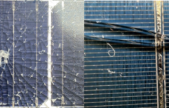
Toshiba’s latest achievement is the development of a new coating method with perovskite layer. Previously, the company developed a two-step coating process in which first a layer of PbI2 (Lead Iodide) ink was applied to a substrate and then a layer of MAI (Methyammonium Iodide, CH3NH3I) ink, which triggered a reaction that formed a MAPbI3 layer. However, this multi-step approach had a slow coating rate and often left unreacted areas in the perovskite layer (Figure 1, left). An alternative is a one-step process in which MAPbI3ink is applied directly, but it is not easy to control the crystallization of MAPbI3 and obtain a uniform perovskite layer over a large area (Figure 1, right). A new coating method was required to address these problems.
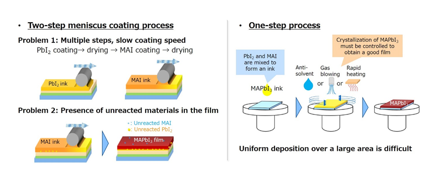
(Right) The problem with the one-step process. (Source: Toshiba)
Toshiba has developed a one-step meniscus coating method that uses improved ink, film drying process, and manufacturing equipment to form a uniform perovskite layer in an area of 703cm2. These innovations halve the perovskite layer deposition steps and increase coating speeds to 6 meters per minute on 5x5cm2modules. This is a speed that meets the requirements for mass production * 3 (Fig. 2, left).
The previously reported one-step meniscus coating method applied to Toshiba’s 703cm2 polymer film-based perovskite photovoltaic module achieved the world’s highest 15.1% PCE for a polymer film-based large-area perovskite photovoltaic module. To do. (Fig. 2, right). This higher PCE and faster and simplified manufacturing process will significantly advance the commercialization of high efficiency, low cost, polymer film based perovskite photovoltaic modules.
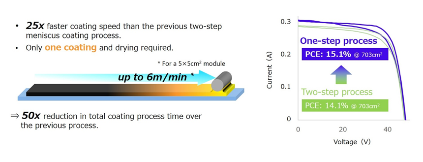
(Right) Current–voltage curve (IV curve) shows PCE raised to 15.1% @ 703cm2 polymer film-based module. (Source: Toshiba)
Toshiba estimates that if installed on a roof area of 164.9 square kilometers, the new perovskite photovoltaic modules will generate electricity equivalent to two-thirds of the annual electricity consumption of households in Tokyo, which is approximately equal to the roof surface area of all buildings in Tokyo.
Toshiba will continue to research perovskite photovoltaic modules, aiming to increase the PCE to 20% or more and expand the effective area to 900cm2, which is the size required for practical applications. The company estimates that achieving these goals will reduce the manufacturing cost of perovskite photovoltaic modules to \15/W (approximately US$0.14/W).
The newly developed coating technology and the perovskite solar modules using this technology are the research results of the New Energy and Industrial Technology Development Organization (NEDO) project “Promoting the development of technology for photovoltaic power generation as the main power source”.


