

1.Introduction
LONGi Green Energy Technology Co, Ltd entered into a global, non-exclusive, cross-licensing agreement with Shin-Etsu Chemical Co, Ltd on March 25, 2020. As a result of the agreement, any application of LONGi products that relates to Gallium-doped technology will be permitted legally on a global basis. Gallium-doped silicon can effectively solve LID (Light induced degradation) in a P-type PERC module. LONGi already addressed the problem of the high cost of Gallium-doped silicon through its own technological efforts and will therefore now be able to provide this for the whole PV industry. At the same time, LONGi commits to the price of Gallium-doped silicon being the same as that for Boron-doped silicon, which will further help PV become the most cost-effective method of power generation.
2.Literature review of Gallium-doped and Boron-doped silicon
Today’s industry-standard Boron-doped monocrystalline silicon still suffers from LID over its lifetime. Industrial Czochralski (Cz) silicon contains significant amounts of interstitial oxygen which, in combination with Boron-doping, can result in LID and, in turn, affect cell efficiency. To our knowledge, the first observation of LID in non-particle-irradiated solar cells fabricated on boron-doped Cz-Si wafers was made by Fischer and Pschunder in 1973 [1]. They recorded a strong degradation of short-circuit current and open-circuit voltage during the first hours of illumination until a stable level was reached. Interestingly, the initial cell performance could be completely recovered by a low temperature anneal at only 200°C. Additional photoconductance decay measurements indicated that the observed effect was due to a bulk carrier lifetime varying between two levels, corresponding to two different states of the material, A and B. State A is associated with a high lifetime and requires low-temperature annealing, while state B is associated with a low carrier lifetime and is caused by illumination. Both levels were found to have a tendency to saturate which can be reversed by applying the appropriate treatment.
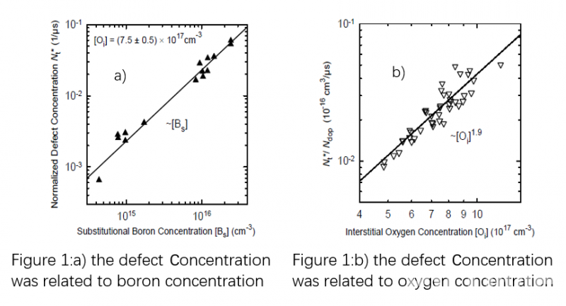
Over the following few years, several attempts were made to develop a defect model which explained the mechanism of LID. Some of them proposed the mechanism of metallic impurities, but none of the models were capable of explaining the complete degradation/recovery cycle observed in Boron-doped Cz silicon. It was not until a complete defect reaction model proposed by Jan Schmidt [2], which did not involve any metallic impurities, that one existed capable of explaining the lifetime degradation under illumination (or minority-carrier injection in the dark) as well as the lifetime recovery during annealing at temperatures above ~200°C. In 2004 Jan Schmidt carried out further research on the boron oxygen defect. It was found that the defect concentration is directly proportional to the boron concentration and squared to the interstitial oxygen concentration [3], as can be seen in figure 1.
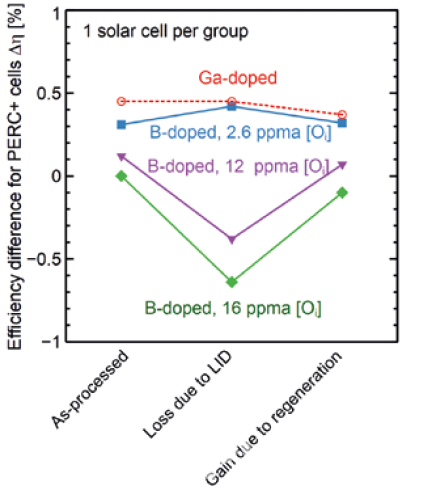
Therefore, two straightforward methods to eliminate the LID are either the reduction of interstitial oxygen content or substitution of the boron by a different dopant (e.g., by Gallium). Bianca from ISFH and Yichun Wang from LONGi [4] jointly carried out research and found that Cz silicon with low oxygen content or Gallium doping had a better anti-LID performance. However, PERC solar cells from industrial Boron-doped Cz silicon with oxygen content of 12 ppm and 16 ppm degraded by 0.5% and 0.7% respectively, as can be seen in figure 2.
Fabricating industrial Boron-doped Cz silicon with low oxygen content (e.g., 2.6 ppm) is very difficult. Technologically, it can be achieved by magnetically-confined Czochralski (MCz) crystal growth. However, due to the application of a strong magnetic field, machine costs are significantly higher when compared to commonly used Cz pullers. Therefore, using Gallium as a dopant becomes a feasible way to solve the LID problem. Since the resistivity distribution of silicon wafers will affect the cell efficiency, A. Metz studied the relationship between wafer resistivity and cell efficiency [5] in figure 3.
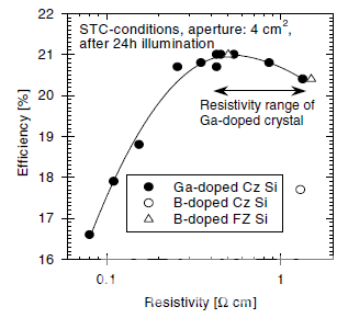
Peak efficiency of up to 21% has been achieved on 0.4Ωcm material. In the relatively broad resistivity range from 0.25 to 1.34Ωcm, cell efficiency can reach more than 97% of the peak value, suggesting that the resistivity of Gallium-doped silicon wafers should be based on this result in order to achieve maximum cell efficiency.
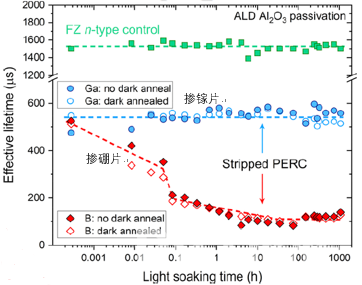
In recent years, light and elevated temperature induced degradation (LeTID) has been observed in multicrystalline, float-zone and Cz silicon. It involves an initial lifetime degradation, but typically recovers over time, with degradation and recovery rates depending on thermal history. Nicholas E. Grant [6] found that LeTID exists in both Gallium-doped and Boron-doped monocrystalline silicon wafers (figure 4.)
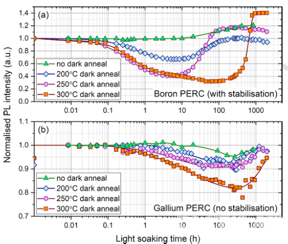
In the same annealing conditions, the degradation of a Gallium-doped PERC cell is lower than that of a Boron-doped equivalent. For further analysis of the bulk lifetime degradation of Gallium-doped and Boron-doped silicon, eliminating the influence of surface metallization of the silicon wafer, the Gallium and Boron PERC cells were stripped and passivated by ALD Al2O3, resulting in a complete change in degradation characteristics, with no degradation for Gallium and boron-oxygen-like degradation for Boron in figure 5.
According to a research report by the University of New South Wales [7], LeTID is caused by a complex combination of several metallic impurities and hydrogen. By controlling the concentration of hydrogen, LeTID can be effectively inhibited. When using Gallium-doped silicon, since there is no need to introduce too much hydrogen for passivating the boron and oxygen defects, LeTID can be easily controlled.
3.The basic property of LONGi’s Gallium-doped silicon wafer
The specifications of LONGi’s Gallium-doped silicon wafer are shown in table 1. All indexes in the table are tested according to GB/T 25076-2018 《Monocrystalline silicon wafer for solar cells》.
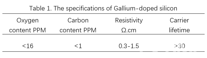
The difficulty in application of Gallium-doped silicon wafers resides in the control of resistivity compared with Boron-doped silicon, since there is a significant difference between the segregation coefficient of Boron (0.75) and Gallium (0.008). LONGi’s R&D focuses on the characteristics of Gallium-doped silicon, in order to achieve a reasonable resistivity range and higher doping accuracy. The objective is to improve the Gallium-doping process via an innovative model which controls the resistivity range from 0.3 to 1.5 Ω.cm, which is almost the same as that for Boron-doped silicon.
LONGi can also provide corresponding resistivity products according to customer demand, in which it is able to reduce the probability of different brightness in EL images on cells. Moreover, the oxygen and carbon content and carrier lifetime of LONGi’s Gallium-doped silicon wafers are basically the same as for Boron-doped products.
Compared with a Boron-doped silicon wafer, Gallium-doped silicon avoids the LID caused by a boron-oxygen defect. As long as the hydrogen content in the cell production process is controlled, LeTID can be inhibited and the total degradation of both cell and module will be very low.
4.The application of Gallium-doped silicon
LONGi’s Gallium-doped silicon wafer has been verified by a number of cell manufacturers, its efficiency and anti-PID performance showing an improvement when compared to a Boron-doped cell.
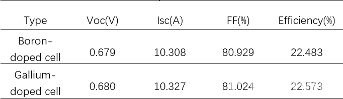
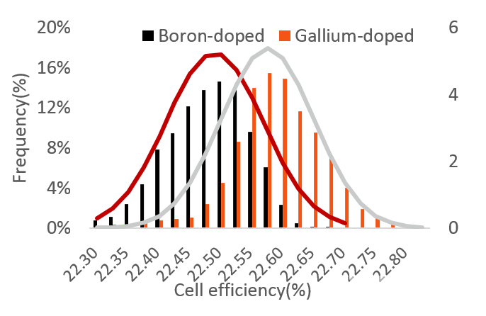
The test results for LONGi cells are shown in table 2 and figure 6. The average efficiency of Gallium-doped cells is 0.09% higher than that of Boron-doped equivalents.
Aiko Solar has carried out testing on Gallium and Boron-doped cells, including an efficiency test where 5kWh LID (Irradiance is 900-1100W/ m2, test temperature is 55-65°C) and CID (110° 0.5A 8hours),as can be seen in table 3. It was found that Gallium-doped cells had better anti-degradation performance than Boron-doped equivalents.
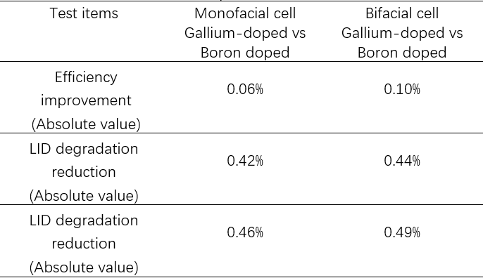
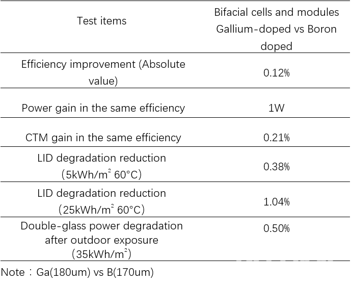
Chint Global carried out further research on the relative performance of Gallium- and Boron-doped cells and modules, as can be seen in table 4. The Gallium-doped silicon wafer performed very well, both in cell and module applications. Cell manufacturers do not require configuration of illumination or electrical injection regeneration process equipment. From the quality control point of view, this method of solving LID at the material side is more reliable than at the process side (eg illumination and electrical regeneration process).
5.Summary
In summary, Gallium-doped PERC cells have a higher efficiency and better anti-LID and anti-LeTID performance compared with Boron-doped cells. LONGi will promote its Gallium-doped silicon wafers for the whole industry chain, making a significant contribution to a reduction in initial module degradation, lowering equipment costs for cell manufacturers and increasing profits for the whole PV industry.
References:
1.Fischer, H. & Pschunder, W. 1973, “Investigation of photon and thermal induced changes in silicon solar cells”, Proc. 10th IEEE PVSC, Palo Alto, California, USA, p. 404
2.J. Schmidt, A.G. Aberle, and R. Hezel, Proc. 26th IEEE Photovolt. Spec. Conf. (IEEE, New York,1997), p. 13.
3.J. Schmidt, Physical Review B, 69(2004) 024107.
4.Binaca Lim, “Beyond boron–oxygen deactivation: Industrially feasible LID-free p-type Czochralski silicon”, LID mitigation | Cell Processing.
5.A. Metz, J. Schmidt, A.G. Aberle, and R. Hezel, Proc. 26th IEEE Photovolt. Spec. Conf. (IEEE, New York,1997), p. 13.
6.Nicholas E. Grant, “Lifetime instabilities in gallium doped monocrystalline PERC silicon solar cells”, Solar Energy Materials and Solar Cells. 7.Daniel Chen, “A Current Perspective on Light-and Elevated Temperature-Induced Degradation (LeTID): Defect Mitigation, Models and Root Cause”, 15thChina SoG Silicon and PV Power Conference.

